Critical Embedded Systems are everywhere . . . Become a leader in setting new directions! |
VMEbus Read/Write Cycles
The VMEbus read/write cycle is the 'standard' bus cycle. It has the following attributes:
- It's the 'basic' data transfer cycle.
- 8, 16, 24 or 32 bits of data can be transferred during each cycle.
- 64 bits of data cannot be transferred with the read/write cycle.
- 16, 24 or 32 bit addressing can be used.
- 40 and 64 bit addresses cannot be used with a read/write cycle.
Table 1 shows the VMEbus signals that are used by the read/write cycle. They are grouped as address, data and control type signals.
|
|
||
|
|
|
|
|
AM0-AM5 DS0*, DS1* LWORD* |
|
WRITE* DS0*, DS1* DTACK* BERR* RETRY* |
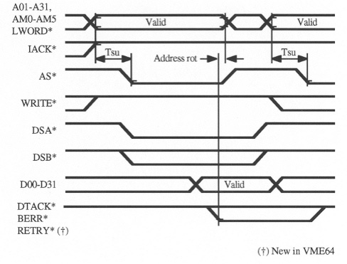
Figure 1 shows a typical read cycle (with address pipelining). During that cycle, the following activity occurs:
- The MASTER drives address (A01-A31), address modifier (AM0-AM5) and LWORD*. This indicates which SLAVE should respond to the cycle.
- The MASTER negates IACK*, to indicate that it is not an interrupt acknowledge cycle.
- The MASTER asserts address strobe AS* to indicate that a valid address is present.
- The MASTER negates WRITE* to indicate that a read cycle is present.
- The MASTER asserts one or both data strobes DS0*, DS1* to indicate where on data bus D00-D31 it will expect to read data.
- After some interval, the SLAVE drives data bus D00-D31.
- After the data bus is stable, the SLAVE asserts data transfer acknowledge (DTACK*). Alternatively, the SLAVE can also assert bus error (BERR*) to indicate that an error (such as a parity error) has occurred during the cycle, or it can assert retry (RETRY*) to indicate that the SLAVE is busy (so that the MASTER retries the cycle at a later time).
- After some interval, the MASTER latches the data on D00-D31.
- The MASTER negates DS0*/DS1* to indicate that it has latched the data.
- The SLAVE negates DTACK* to indicate that it has finished with the cycle.

Figure 1. Read cycle with address pipelining.
The VMEbus write cycle is not shown. It is similar to the read cycle, except that the MASTER asserts WRITE* and places valid data onto the bus. The SLAVE then latches the data after DSA* has been asserted by the MASTER.
Data Strobe Nomenclature
It should also be noted that the VMEbus specification uses two forms of nomenclature for the data strobes. The actual signal names are called DS0* and DS1*. However, the specification often refers to data strobes DSA* and DSB*. These are not the names of actual signal lines, but are used to indicate the order in which the data strobes are asserted. DSA* is always driven first by the MASTER, and DSB* is always driven second. However, DSA* can refer to either DS0* or DS1*. Also, in some cases the term DSX* can be used. This is shorthand notation which indicates that either data strobe is asserted.
Interlocked Bus Cycles
VMEbus uses a fully interlocked handshaking mechanism between data strobes DS0* and DS1*, and terminating signals DTACK*, BERR* and RETRY*.
At the beginning of a cycle a MASTER must not assert either data strobe until DTACK*, BERR* and RETRY* have all been negated by the SLAVE. Failing to do so may corrupt data on the current (or the previous) cycle. At the end of a cycle a SLAVE cannot negate DTACK*, BERR* or RETRY* until the MASTER has negated both data strobes DS0* and DS1*. These two mechanisms form a fully interlocked handshaking mechanism.
Care must be used when evaluating or designing MASTERs that use the 680XX or other microprocessor families. Many microprocessors don't use a fully interlocking bus cycle, and circuitry must be provided to make them totally compliant.
Address Pipelining
Some microprocessors or peripherals use address pipelining to speed up data transfers. During address pipelining the bus master broadcasts the address of the next bus cycle before the current cycle has completed. This is shown as 'address rot' (i.e. a rotten address) in Figure 1. There, the MASTER places a new address onto the bus immediately after the SLAVE asserts DTACK*. However, this can take place before the SLAVE negates the DTACK* signal.
Originally, address pipelining was considered a VMEbus feature. However, on rare occasions it has caused incompatibility between modules. In those cases, a poorly designed VMEbus SLAVE module will latch it's address lines on the falling edge of AS*. This can cause problems if the MASTER is attempting an address pipelining cycle. In those cases, the MASTER can latch the wrong data, thereby corrupting the bus cycle. If the SLAVE is designed correctly, however, this problem will not occur.
This page last updated: Dec 5, 2000
Copyright 2000 Wade D. Peterson. All rights reserved.
